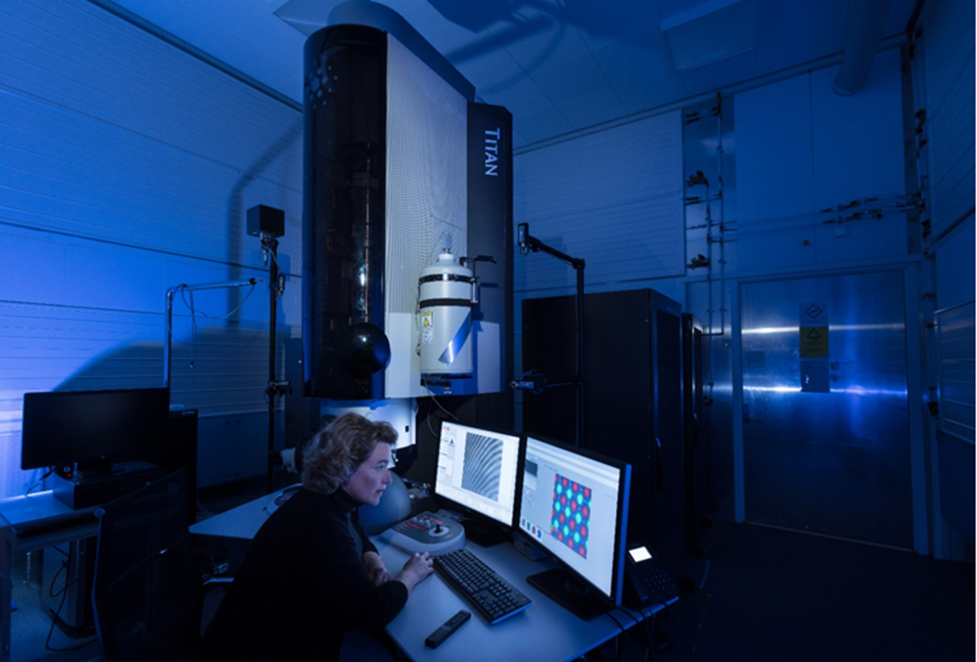
Transmission Electron Spectroscopy (TEM)
Contact person

In transmission electron microscopy, a high energy electron beam (60 – 300 kV) is transmitted through a thin sample (less than 100 nm thin). The electrons are scattered elastically (not losing energy) and inelastically, providing us with information about the atomic and electronic structure, particles, grain boundaries, defects and surface structures, as well as chemical elements present.
High Resolution TEM (HRTEM)
This imaging technique provides atomic resolution for crystalline materials. From HRTEM images you can get information on the crystalline structure, defects, grain boundaries, particle shape/structure/distribution, and you can map strain in your sample.
Scanning TEM (STEM)
Imaging your sample in STEM mode, provides you with images of your sample from several detectors at different scattering angles. This mans that electrons that are scattered mostly elastically (forward scattering), by very light elements or thin regions will be detected with a bright field detector. While electrons that are being scattered by heavy elements will be scattered further out, onto the high angled annular dark field detector (HAADF). This is what we call z-contrast imaging. The contrast of the image is dependent on the atomic number of the elements in your sample. This technique uses a fine probe that scans the surface of your sample. This will give you very local information in each pixel. Combining this EELS can give you an EELS spectrum in each pixel, EELS-spectrum image, a cubed data box.
Electron Diffraction (ED)
When electrons are scattered elastically through the sample, electron diffraction patterns are created in the back focal plane of the objective lens of the microscope, ED provides information about the crystalline structure and symmetry of the atomic packing. It can also provide information on preferred crystallographic orientations, as well as on defects.
Energy Dispersive X-ray Spectroscopy (EDS)
When the electrons are scattered inelastically by the sample, the electron beam can excite core electrons to unoccupied states. When they fall back to their original position, they emit an X-ray. This X-ray can then be detected and are characteristic for that particular element. These X-rays can be used to map the elements present in the sample at the atomic scale. This technique works best with heavier elements.
Electron Energy Loss Spectroscopy (EELS)
We can measure the amount of energy that the electrons have lost when passing through the sample. These energy losses are, as with EDS, characteristic for that particular element, and can be compared to the peaks in XPS (LINK). In the EELS spectra there is a huge amount of information that can be extracted. A few of these are information about the chemical composition, surface and bulk plasmons, size of band gap, fine structure, coordination, binding energy, oxidation state and magnetic properties.
Relevant links
Infrastructure networks:
Projects:
