

The researchers and engineers at MiNaLab are working to bridge the gap between applied research, innovation, and production.
In the green transition, it is crucial to research relevant technology that can be quickly adopted.
No green transition without digitalization, no digitalization without microchips.
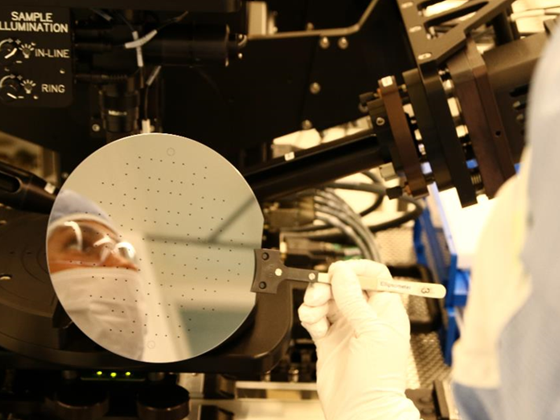
At SINTEF MiNaLab, everything is done from idea to production. This is the only independent, complete line for the development and fabrication of microchips in Norway.
This includes everything from basic research to the development of production processes, design, and production. MiNaLab also contributes to education.
Read more about our development of piezoelectric MEMS here.

Facts about MiNaLab:
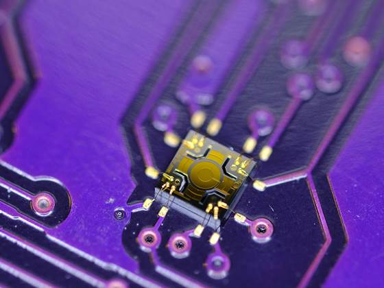
- Specialized expertise in producing sensors that can measure pressure underwater, in the air, and in space.
- Approximately 20 companies, both national and international, depend on microchips made at MiNaLab. In addition, MiNaLab is a development partner for about 20 companies.
- Collaborates with Norwegian companies, half of which are startups. In total, this involves about 300 Norwegian jobs.
- Develops and delivers specially designed sensors, which are not off-the-shelf items. These are components that give Norwegian and European companies unique competitive advantages.
SINTEF MiNaLab's main focus is on sensor chips. Sensors will be instrumental in digitalization, and thus also in the green transition.
- MiNaLab is part of NorFab, a national partnership of infrastructure for micro- and nanofabrication in Norway. They are located in Vestfold, Oslo, and Trondheim.
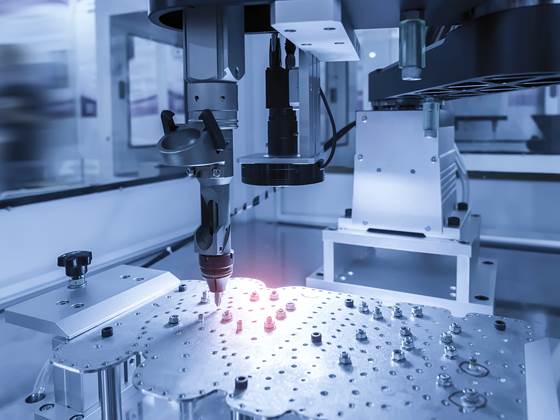
The lab has a high-tech cleanroom of 800 sqm, is certified according to ISO 9001:2015 (quality management), ISO 14001:2015 (environmental management), and ISO 45001 (occupational health and safety). It is organized under the Department of Microsystems and Nanotechnology at SINTEF Digital.
Both Norwegian and international industry use SINTEF MiNaLab for the production of key components.