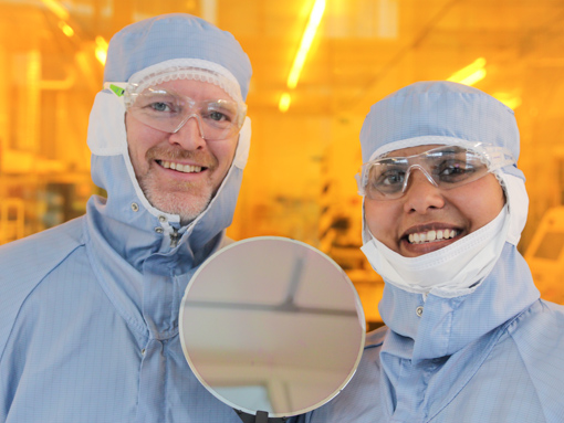
SINTEF MiNaLab has worked with design, modelling and fabrication of piezoelectric microsystems on 150 mm wafers including materials development of piezoelectric thin films by CSD, PLD and sputtering since 2003.

SINTEF MiNaLab lowers the entry barrier for this technology by offering assistance in areas specific to piezoelectric MEMS such as design, modelling, thin film deposition, small-scale prototyping. SINTEF's deposition processes and device processing are on pre-production level. This will lower the risk in your project.
SINTEF MiNaLab is a member of The Centre for Dielectrics and Piezoelectrics.
Read more about how SINTEF MiNaLab can contribute to your project on piezomems.com